Geneve wait state generation
Architecture
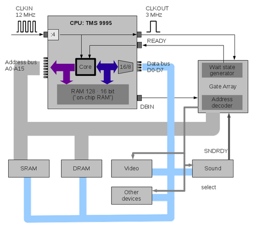
This is a simplified schematic of the addressing mechanism in the Geneve.
The CPU, the TMS 9995, contains an own set of memory locations at addresses >F000 to >F0FB and the remaining 4 bytes at the end of the address space, that is, >FFFC to >FFFF (which are the NMI branch vector). The internal memory locations are directly connected to the 16 bit data bus, so we should say these are 128 words of 16 bit each.
All other memory locations are outside of the CPU, and the 16 bit data transfers are converted to a sequence of two 8 bit data transfers. This is quite similar to the mechanism used in the TI-99/4A, with the exception that the TI send the odd address byte first, then the even address, and the TMS 9995 starts with the even address, followed by the odd address.
Wait states can only be created outside of the CPU; there is no way of creating wait states within the CPU (possibly also no need). There is a special PIN called READY which is used for wait state creation.
Instead, we have an external wait state generation. The gate array circuit is used to create wait states in certain situations. When a wait state shall appear, the READY line of the CPU must be pulled down (cleared).
One wait state has the exact duration of one cycle which is 333.3 nanoseconds. Three millions of them last for one second.
Apart from the permanent wait state, the CPU itself does not create any wait state. This should be considered when only internal accesses are done: If code is running within the internal CPU RAM, wait states have no effect. They have only effect for external memory accesses.
Timing diagrams
Some diagrams may help to understand the concept of wait states on the Geneve. I picked some of the lines, but there are some more, also important ones. If you are interested in the exact set of signal lines please see the TMS9995 specification. For now, we only discuss waitstate generation.
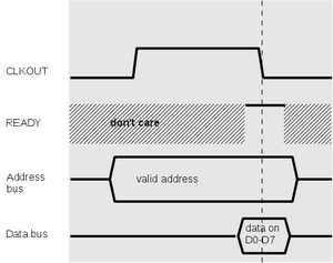
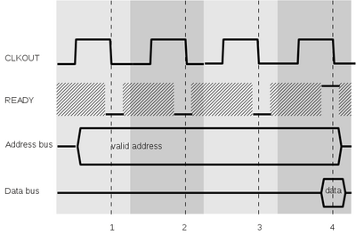
This is the timing diagram for reading from external memory.
A read operation starts with the address lines (A0-A15) being set to some value. For example, when the CPU wants to read from >1000, A3 is set to 1 while the remaining address lines are set to 0.
Next we expect that the device (like RAM, video, etc.) puts the value of the given address on the data bus. Depending on the device, the requested data may be available after some delay time, or the lines may be unstable until that time has passed. The CPU waits for the falling edge of the CLKOUT signal. At that point it first checks the READY line, and if it is high as shown here, the data lines are sampled, and the memory read access is complete. After that the program counter is increased and the next access may start.
Notice that the READY line may have any value (0 or 1) at other times; we symbolize this with the hashed stripe.
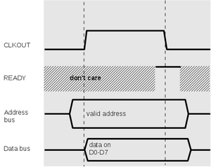
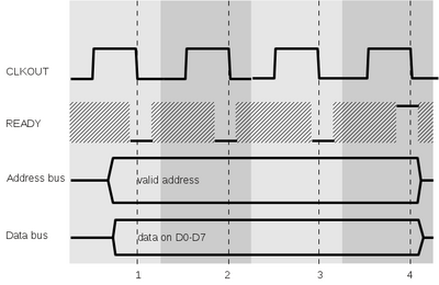
For writing the diagram looks a bit different, but still familiar. Again we omit some lines like WE line (write enable) for now. Different to reading, the writing process requires that the data bus be set shortly after the address is set. This is clear, since we must assume that the addressed device immediately fetches the values once the address is set. The CPU has no influence on the behavior of the device.
The external device may require some more time before the processing can continue; in this case it may lower the READY line; the CPU will test the line on the next falling CLKOUT edge. When it is high, as shown here, the memory write is complete, and the CPU continues with the next cycle, advancing the program counter. Remember that the CPU ignores the READY line when the memory access was directed to the internal memory locations, so in that case, the memory access is always complete at the end of the cycle.
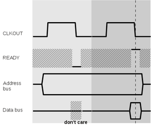
Now we have a look at the situation when a wait state is inserted. Here, a read operation is delayed by one cycle; this is typically the case when the Geneve uses its DRAM.
The memory read access starts as above, but at the first CLKOUT falling edge, the READY line is low. Now if this read access is actually an external access (and not to the on-chip RAM), the CPU skips the sampling of the data bus and waits for another falling CLKOUT edge. At that point we are at the same situation as above, and the access is complete.
What happens if we have multiple wait states? On the left side we can see a read access; as expected, the CPU loops until the READY line is high, and at that point it reads the values from the data bus. When writing, the CPU again attempts to assign the values shortly after the rising edge of CLKOUT, which is also used by the external device as the moment after which data may be safely read. The external device pulls down the READY line for this and another two cycles. This causes the CPU to loop until it finds a high READY level.
DRAM access
For each DRAM access, the gate array creates 1 wait state. That means that for word accesses (like CLR or MOV), two wait states will be created. If the operation and both word operands are in DRAM, we get at least 6 wait states which can have a significant impact on performance.
SRAM accesses are, by design, zero wait state accesses. Word operations in the SRAM are still slower than in the internal CPU RAM, since the internal RAM is organized as 128 words of 16 bits, so writing a word only takes one cycle, while it takes two cycles for the external memory which is connected on the 8-bit data bus.
Memory access
We can use software to turn on additional wait states for memory access using the flag bit at CRU address 1EFE. When active (low), wait states are created on every external memory access, either reading or writing. For CPU RAM accesses (memory locations F000 to F0FB) no wait states are created.
Some things should be considered:
- For each external memory access, 2 wait state cycles are created. This means that for word operations, 4 wait states are produced.
- Wait states created by this method do not add on the DRAM wait states. Here, memory operations in SRAM and DRAM work at the same speed.
- For calculating the total number of cycles spent with one operation, the number of memory accesses for determining the source and destination memory location must be considered. In particular, the address calculation may be quite easy when registers are used, and very complex when the contents of a register must first be read and then added to a value which must be read from the following memory location.
Assumung that the following line and the registers reside in CPU RAM, the instruction
MOV R2,R3
takes three cycles (read MOV (including the values 2 and 3), read value at location of R2, write value to location of R3). This does not change when wait states are active. In contrast,
MOV @SRAMLOC,@SRAMLOC+2
takes 7 cycles without wait states (read MOV, read SRAMLOC, read SRAMLOC+2, read byte from SRAMLOC, read byte from SRAMLOC+1, write byte to SRAMLOC+2, write byte to SRAMLOC+3) and 15 cycles with wait states (add 2 wait states for each of the last four operations).
Video operation
As known from the TI-99/4A, accesses to the Video Display Processor must be properly timed, since the VDP does not keep up with the higher speed of the CPU. When bytes are written in a too high frequency, some of them may be lost; when reading, the value may not reflect the current video RAM contents. Setting the address may also fail when writing too quickly. All this is a consequence of a missing synchronization link between VDP and CPU. The CPU cannot find out whether the video processor is ready for the next byte. (Note that for V9938 commands, a ready flag is available to determine whether some command has finished processing.)
The problem has become worse with the higher performance of the Geneve. This may mean that programs that worked well with the TI may fail to run on the Geneve because of VDP overruns. For this reason, wait states may be inserted for video operations.
However, there is one thing to remember: Wait states can only be inserted into memory accesses.
This means that if we do not use memory accesses, the wait states are not effective. The access to the VDP ports does not count as an external memery access. If we write a program that resides in CPU RAM completely, operating on the VDP, we cannot slow it down with the wait states. Therefore, video access should not be done from the CPU RAM.
Automatic wait state generation
Within the Geneve, wait states can be generated to slow down operation for keeping timing constraints. The TMS 9995 CPU can create wait states itself on every external memory access by a certain hardware initialization (READY high with RESET going from low to high). This is not used in the Geneve as those wait states cannot be turned off.
